About the WBSL

About the WBSL
The Wide Bandgap Semiconductor Laboratory has had an esteemed history of innovation. Professor Moustakas started the lab in 1987 with the purchase of the Varian GEN II molecular beam epitaxy (MBE) system. It originally focused on the growth of III-nitrides and the study of its fundamental properties. Many significant discoveries have been made about the basic properties and growth control of III-nitrides. Since its conception, the lab has expanded to include an Eiko MBE, two custom-built hydride vapor phase epitaxy systems (one horizontal and one vertical), a sputter deposition system, an electron beam evaporator, and an inductively coupled plasma reactive ion etching (ICP-RIE) system. More recently, the lab's focus has shifted to the development of III-nitride optoelectronic devices, particularly LEDs and lasers.
People
Theodore D. Moustakas
Professor of Electrical & Computer Engineering
Professor of Materials Science & Engineering
Dr. Moustakas is the inaugural Distinguished Professor of Photonics and Optoelectronics at Boston University. He received his PhD from Columbia University in 1974. He held research positions at Harvard University and Exxon Corporate Research Laboratory prior to joining Boston University in 1987 as a Professor of Electrical and Computer Engineering. He is also a Professor of Physics and Associate Head of the Division of Materials Science and Engineering.
Dr. Moustakas's research contributions cover a broad spectrum of topics in opto-electronic materials and devices, including nitride semiconductors, amorphous semiconductors, III-V compounds, diamond thin films and metallic multi-layers. He is the co-editor of eight books, including Gallium Nitride I (Academic Press, 1998) and Gallium Nitride II (academic Press, 1999), the author of chapters in eight books and 340 papers in technical journals and conference proceedings (Google citations 11,550, h index 52). He served as a special editor of the Journal of Vacuum Science and Technology and of the Journal of Electronic Materials. He presented 140 invited and plenary talks in national and international conferences. He has been granted 31 U.S. patents and several are pending in the fields of nitride semiconductors, amorphous silicon and diamond materials. Intellectual property that resulted from his work has been licensed to a number of companies, including major manufacturers and users of blue LEDs and lasers (Cree, Nichia, Philips, OSRAM, Apple, Google, Amazon, Samsung, LG, Sony etc.).
Dr. Moustakas is a Fellow of the American Physical Society (1994), the Electrochemical Society (1997), the Institute of Electrical and Electronic Engineers-IEEE (2014), and a Charter Fellow of the National Academy of Inventors (2012). He holds an honorary doctoral degree from the Aristotle University (2003); he received the MBE Innovator Award in 2010; in 2011 he received the Distinguished Scholar Award from the BU College of Engineering and in 2013 he received the Boston University Innovator of the Year Award.
Denis Nothern
Graduate Student
B.S. Materials Science & Engineering, Cornell University (2007)
M.S. Materials Science & Engineering, University of Michigan (2011)
Design, growth, fabrication, and characterization of deep ultraviolet LEDs.

Research
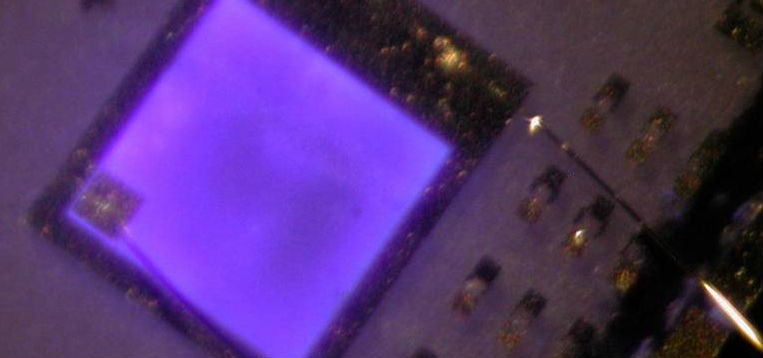
Deep Ultraviolet LEDs
The development of novel high efficiency deep ultraviolet LEDs.

Vitamin D
UV LEDs for treatment of vitamin D deficiency
InGaN QDs
Growth of InGaN QDs
Equipment
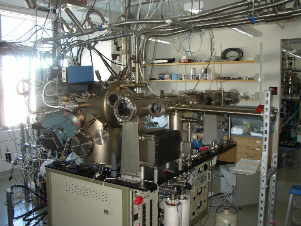
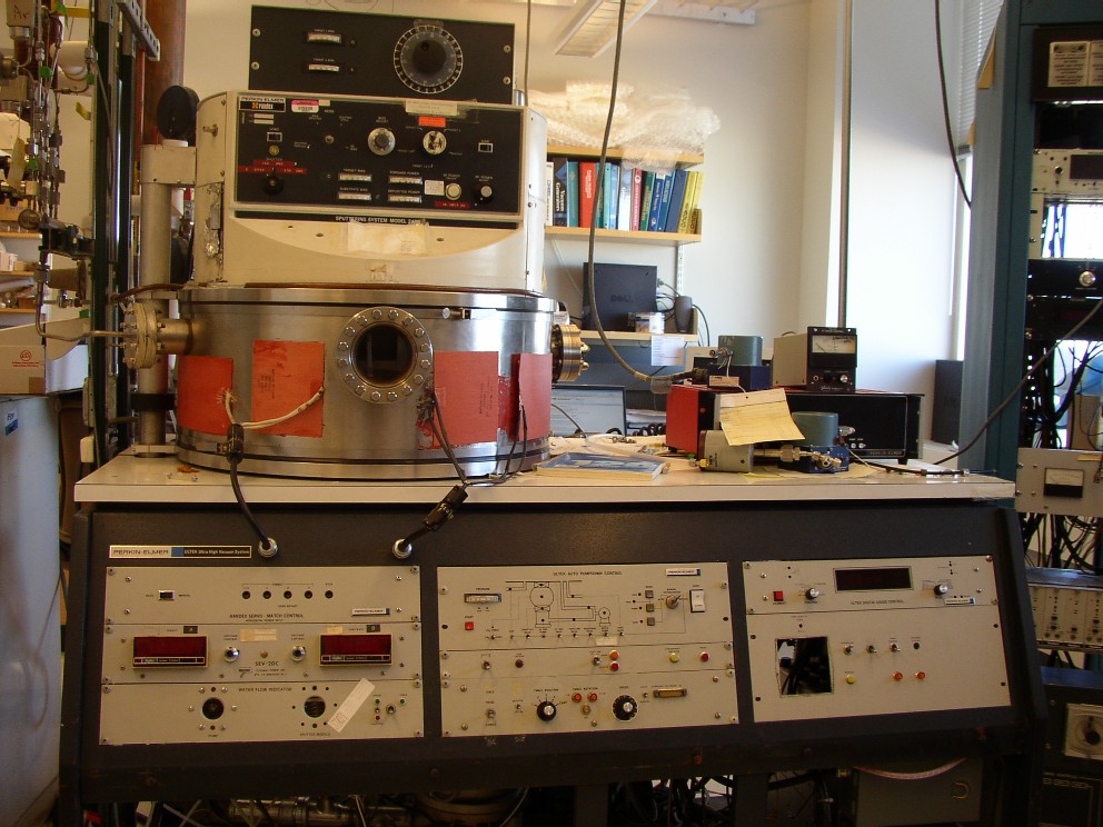
Nitrogen Cluster Source
The nitrogen cluster source is a relatively new technique for MBE growth of nitrides. Because molecular nitrogen gas is not reactive, special steps must be taken to create nitrides. In a traditional plasma assisted MBE system, a nitrogen RF plasma source is used. In this system, clusters of nitrogen atoms are created by injecting high pressure molecular nitrogen into a vacuum chamber through a small nozzle. The rapidly expanding gas forced through a bottleneck creates clusters of nitrogen bonded by Van der Walls forces. Within this vacuum chamber, the clusters are first charged by a tungsten filament, then accelerated towards the sample by a large electric field. The voltage of this field determines the energy of the cluster, which is set to be low enough to not damage the surface of the sample, but sufficient to break the clusters into free nitrogen atoms, which will be reactive.
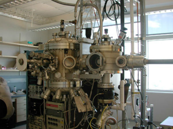
Vertical HVPE
Hydride vapor phase epitaxy is based on passing HCl gas over a heated source of group III material such as gallium or aluminum then reacting it with ammonia gas over the substrate. The advantages of this technique are very low crystal defect densities and growth rates more than 10x faster than MBE. These properties make HVPE excellent for growth of high quality AlN or GaN templates on sapphire. The flow of process gas in this vertically oriented system is not distorted by convection and gravity, thus producing high uniformity.
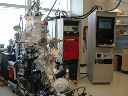
Horizontal HVPE
This horizontal hydride vapor phase epitaxy system is simpler and more compact that its vertical counterpart. The samples are easily mounted on a molybdenum susceptor that is inductively heated as high as 1400° C. A venturi pump is used to reduce the pressure within the reactor to improve uniformity of the process gas flow.
ICP RIE
The inductively coupled plasma reactive ion etcher is used to etch nitride materials which are not otherwise easily etchable. An RF coil generates a plasma in the process gasses (chlorine and argon), and a separate bias voltage is applied to draw the plasma towards the etching target. This arrangement allows for the generation of a high density plasma with a high etch rate that can be precisely controlled.
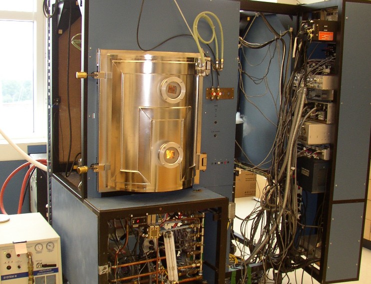
Electron Beam Evaporation
We have an electron beam evaporator for the deposition of metal device contacts and optical films. E-beam evaporation is particularly suitable for the evaporation of high melting point metals and oxides. We can simultaneously deposit on as many as 20 3" wafers mounted on a planetary rotating stage. Gas can be bled into the system during deposition allowing for higher quality oxide films.
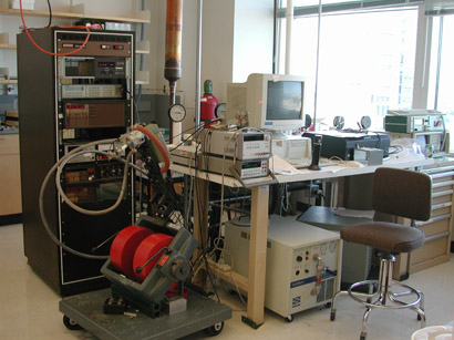
Electrical Characterization
Our Keithley S110 Hall Effect system can be used to measure carrier concentration as well as conductivity in thin films. The system is composed of a Keithely 220 Current Source, 617 Electrometer, 196 Multimeter, and a Quad Electrometer Buffer Amplifier Relay Module. For measuring the current-voltage characteristics of devices we have a Keithley 2420 SourceMeter, an Agilent 8114A Pulse Generator, an HP 54610B Oscilloscope, and a Stanford Research SR830 DSP Lock-In Amplifer.
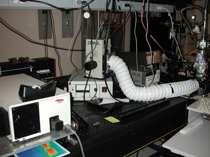
Optical Characterization
Our dark room is equipped with an Acton Research SpectraPro-500 0.5 m monochromater, an Acton Research SpectraPro-300i 0.3 m monochromater, two Ocean Optics Miniature Spectrometers, photomultiplier tubes, an integrating sphere, multiple Janis low temperature cryostats for nitrogen and helium, and an optical microscope. Light sources include a pulsed 1 mJ 337.1 nm nitrogen laser, a 200 mW 325 nm HeCd laser, an 8 mW 375 nm laser diode, a pulsed 0.3 mJ 224 nm HeAg laser, a 35 mW 633 nm HeNe laser, and a broad spectrum Oriel Xenon Lamp. The dark room is setup to perform temperature dependent photoluminescence and photocurrent measurements as well as the measurement of LED emission spectra and efficiency.
Publications